- 您现在的位置:买卖IC网 > Sheet目录2007 > MAX11101EUB+ (Maxim Integrated Products)IC ADC 14BIT SRL 200KSPS 10UMAX
Maxim Integrated Products 2
MAX11101
14-Bit, +5V, 200ksps ADC with 10A Shutdown
AVDD to AGND .......................................................-0.3V to +6V
DVDD to DGND.......................................................-0.3V to +6V
DGND to AGND ...................................................-0.3V to +0.3V
AIN, REF to AGND ............................... -0.3V to (VAVDD + 0.3V)
SCLK, CS to DGND.................................................-0.3V to +6V
DOUT to DGND.................................... -0.3V to (VDVDD + 0.3V)
Maximum Current Into Any Pin ....................................... Q50mA
Continuous Power Dissipation (TA = +70NC)
F
MAX (derate 5.6mW/NC above +70NC) .....................444mW
WLP (derate 16.1mW/NC above +70NC)......1300mW (Note 1)
Operating Temperature Range.......................... -40NC to +85NC
Maximum Junction Temperature.....................................+150NC
Storage Temperature Range............................ -65NC to +150NC
Lead Temperature (FMAX only; soldering, 10s).............+300NC
Soldering Temperature (reflow) ......................................+260NC
ABSOLUTE MAXIMUM RATINGS
Stresses beyond those listed under “Absolute Maximum Ratings” may cause permanent damage to the device. These are stress ratings only, and functional opera-
tion of the device at these or any other conditions beyond those indicated in the operational sections of the specifications is not implied. Exposure to absolute
maximum rating conditions for extended periods may affect device reliability.
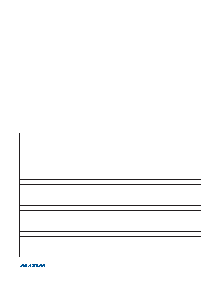
ELECTRICAL CHARACTERISTICS
(VAVDD = VDVDD = 4.75V to 5.25V, fSCLK = 4.8MHz (50% duty cycle), 24 clocks/conversion (200ksps), VREF = 4.096V, TA = TMIN to
TMAX, unless otherwise noted. Typical values are at TA = +25°C.)
Note 1: All WLP devices are 100% production tested at TA = +25NC. Specifications over temperature limits are guaranteed by
design and characterization..
PARAMETER
SYMBOL
CONDITIONS
MIN
TYP
MAX
UNITS
DC ACCURACY (Note 2)
Resolution
14
Bits
Relative Accuracy
INL
(Note 3)
-1
+1
LSB
Differential Nonlinearity
DNL
No missing codes over temperature
-1
±0.5
+1
LSB
Transition Noise
RMS noise
Q
0.32
LSBRMS
Offset Error
0.2
1
mV
Gain Error (Note 4)
Q
0.002
±0.01
%FSR
Offset Drift
0.4
ppm/°C
Gain Drift (Note 4)
0.2
ppm/°C
DYNAMIC SPECIFICATIONS (1kHz sine wave, 4.096VP-P) (Note 2)
Signal-to-Noise Plus Distortion
SINAD
81
84
dB
Signal-to-Noise Ratio
SNR
82
84
dB
Total Harmonic Distortion
THD
-99
-86
dB
Spurious-Free Dynamic Range
SFDR
87
101
dB
Full-Power Bandwidth
-3dB point
4
MHz
Full-Linear Bandwidth
SINAD > 81dB
20
kHz
CONVERSION RATE
Conversion Time
tCONV
(Note 5)
5
240
F
s
Serial Clock Frequency
fSCLK
0.1
4.8
MHz
Aperture Delay
15
ns
Aperture Jitter
< 50
ps
Sample Rate
fS
fSCLK/24
200
ksps
Track/Hold Acquisition Time
tACQ
1.1
F
s
发布紧急采购,3分钟左右您将得到回复。
相关PDF资料
MAX11102AUB+
IC ADC 12BIT SPI/SRL 10UMAX-EP
MAX1111CPE+
IC ADC 8BIT LP 16-DIP
MAX1113CPE+
IC ADC 8BIT LP 16-DIP
MAX1116EKA+T
IC ADC 8BIT SERIAL SOT23-8
MAX11201BEUB+T
IC ADC 24BIT SRL 13.75SPS 10UMAX
MAX11202BEUB+T
IC ADC 24BIT SRL 13.75SPS 10UMAX
MAX11210EEE+T
ADC 24BIT 4WIRE SPI 16-QSOP
MAX11212BEUB+T
IC ADC 18BIT SRL 13.75SPS 10UMAX
相关代理商/技术参数
MAX11101EUB+T
功能描述:模数转换器 - ADC 14-Bit 5V 200ksps w/10uA Shutdown RoHS:否 制造商:Texas Instruments 通道数量:2 结构:Sigma-Delta 转换速率:125 SPs to 8 KSPs 分辨率:24 bit 输入类型:Differential 信噪比:107 dB 接口类型:SPI 工作电源电压:1.7 V to 3.6 V, 2.7 V to 5.25 V 最大工作温度:+ 85 C 安装风格:SMD/SMT 封装 / 箱体:VQFN-32
MAX11101EWC
制造商:MAXIM 制造商全称:Maxim Integrated Products 功能描述:14-Bit, +5V, 200ksps ADC with 10μA Shutdown
MAX11101EWC+
制造商:MAXIM 制造商全称:Maxim Integrated Products 功能描述:14-Bit, 5V, 200ksps ADC with 10??A Shutdown
MAX11101EWC+T
功能描述:模数转换器 - ADC 14-Bit 5V 200ksps w/10uA Shutdown RoHS:否 制造商:Texas Instruments 通道数量:2 结构:Sigma-Delta 转换速率:125 SPs to 8 KSPs 分辨率:24 bit 输入类型:Differential 信噪比:107 dB 接口类型:SPI 工作电源电压:1.7 V to 3.6 V, 2.7 V to 5.25 V 最大工作温度:+ 85 C 安装风格:SMD/SMT 封装 / 箱体:VQFN-32
MAX11102
制造商:MAXIM 制造商全称:Maxim Integrated Products 功能描述:2Msps/3Msps, Low-Power, Serial 12-/10-/8-Bit ADCs
MAX11102_11
制造商:MAXIM 制造商全称:Maxim Integrated Products 功能描述:2Msps/3Msps, Low-Power, Serial 12-/10-/8-Bit ADCs 2.2V to 3.6V Supply Voltage
MAX11102_1108
制造商:MAXIM 制造商全称:Maxim Integrated Products 功能描述:2Msps/3Msps, Low-Power, Serial 12-/10-/8-Bit ADCs
MAX11102ATB
制造商:MAXIM 制造商全称:Maxim Integrated Products 功能描述:2Msps/3Msps, Low-Power, Serial 12-/10-/8-Bit ADCs 2.2V to 3.6V Supply Voltage